Your Partner for Safe and Secure DataBus Solutions
Sital Technology: Leading the Way in Communication Bus Innovation
Sital Technology (Founded in 1997) is a World Wide Leading Provider Of Smart, Robust, and Reliable Communication Bus Solutions For the Avionics, Aerospace, and Automotive Industries. Sital Technology's Airborne Interface Cards and Testers, High-Reliability Components and State-Of-The-Art IP cores including our unique BC Firewall Solution For MIL-STD-1553, EBR-1553, ARINC-429, ARINC-825, CAN and Space Grade IP Are Trusted in 1,000's of Military, Aerospace and Automotive Applications.Fastest Time to Market with 1553 Integration Solutions!Sital Technology Also Has The Fastest Time To Market 1553 Integration Solution !
SITAL Products Are Made In The U.S.A. To Adhere To ITAR Regulations And Strengthen The Supply Chain For Unparalleled Support and Delivery Times.
About Sital
Sital’s mission is to provide safe & secure DataBus Communication Solutions.
Our worldwide customers rely on Sital’s novelty to resolve the most challenging DataBus problems while optimizing production, quality, and cost.
What is 1553? Understanding the Standard
MIL-STD-1553 is a military standard that defines the mechanical, electrical, and functional characteristics of a serial data bus. It was originally designed for the robust, reliable digital information exchange between avionics systems. Sital Technology leverages this standard to offer advanced communication solutions. We guarantee our products meet the rigorous demands of aerospace, automotive, and defense applications.
Sital offers the best-in-class IP cores for 1553 and specializes in integrated FPGA solutions. Our IP cores can work with any FPGA and are designed for accelerated processing. They are highly parallelized, allowing for multiple operations to be executed simultaneously. Our IP cores’ high compliance and efficient FPGA integration make Sital’s FPGA solutions the fastest in the market.

Sital's Best Selling Solutions
For over 25 years, we have been developing reliable products proudly made in the USA.
Our products have been tested in the operational field under the strictest conditions.
We work closely with our partners to meet your needs. We have AMD/Xilinx and Lattice on board to provide turnkey FPGA/MCU design solutions. Micross for their reliable components, as well as Logicircuit and ConsuNova to equip us with DO-254 and DO-178 artifacts for your hardware and software development.
Together, our services are extensive to develop custom solutions based on your needs.
Sital’s Advanced DataBus Fault Finder
Sital’s “SnS” Technology is indispensable for identifying and diagnosing faults in complex DataBus networks, including MIL-STD-1553, CAN, and other critical communication buses. This technology offers ongoing, real-time detection and pinpointing of intermittent or continuous open or short circuit faults in various components such as data bus cables, bus couplers, connectors, stubs, LRUs, and bus terminators.
Whether it’s intermittent faults, signal integrity issues, or complete system failures, our solutions are designed to pinpoint the root cause quickly and accurately.
This capability not only reduces downtime but also ensures the robustness and reliability of your systems. It reflects Sital’s commitment to providing smart, robust, and affordable solutions for high-reliability communication buses.
Click on the type of the product you are looking for:
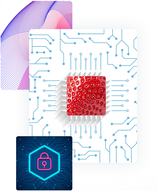
Safe and Secure DataBus Solutions
Sital’s cutting-edge, innovative “SnS” Technology is designed for IP Core’s physical layer. Our solutions offer unprecedented cyber security and DataBus fault finder capabilities.
We supply our products with DO-254 and DO-178 certifiability, including DAL A. Our partners: Logicircuit and ConsuNova provide the DO-254 and DO-178 artifacts. Through enhanced physical layer monitoring, the patented “SnS” analyzes all DataBus messages and provides 2 unique capabilities.

2024©All rights reserved
